N Type Vs P Type Semiconductor
Muz Play
Mar 21, 2025 · 6 min read
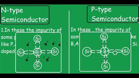
Table of Contents
N-Type vs. P-Type Semiconductor: A Deep Dive into the Fundamentals
The world of electronics hinges on the remarkable properties of semiconductors. These materials, neither fully conductive like metals nor fully insulating like ceramics, form the backbone of modern technology, powering everything from smartphones to satellites. Crucial to understanding semiconductors is the distinction between N-type and P-type materials. This difference stems from the carefully controlled introduction of impurities, a process known as doping, which dramatically alters their electrical behavior. This article will delve deep into the intricacies of N-type and P-type semiconductors, exploring their fundamental characteristics, doping processes, applications, and the pivotal role they play in creating semiconductor devices.
Understanding the Basics: Intrinsic Semiconductors
Before diving into the differences between N-type and P-type semiconductors, it's essential to understand the behavior of an intrinsic semiconductor – a pure semiconductor material without any significant dopant impurities. Silicon (Si) and Germanium (Ge) are common examples. In an intrinsic semiconductor:
-
Covalent Bonding: Atoms are bonded together through covalent bonds, sharing electrons to achieve a stable electron configuration. At absolute zero temperature, all electrons are tightly bound, and the material acts as an insulator.
-
Band Gap: A crucial characteristic is the band gap – the energy difference between the valence band (where electrons are bound) and the conduction band (where electrons are free to move). Electrons require sufficient energy to jump the band gap and become mobile charge carriers.
-
Thermal Excitation: At room temperature, some electrons gain enough thermal energy to overcome the band gap, leaving behind "holes" – the absence of an electron in the valence band. These electrons in the conduction band and the holes in the valence band contribute to the semiconductor's minimal conductivity. This intrinsic conductivity is typically low.
N-Type Semiconductors: An Excess of Electrons
N-type semiconductors are created by doping an intrinsic semiconductor with pentavalent impurity atoms – atoms with five valence electrons, such as phosphorus (P), arsenic (As), or antimony (Sb). These pentavalent atoms replace some silicon atoms in the crystal lattice. Four of their valence electrons participate in covalent bonding with the surrounding silicon atoms. However, the fifth electron is loosely bound and easily becomes a free electron in the conduction band.
Key Characteristics of N-Type Semiconductors:
-
Majority Carriers: The majority charge carriers in N-type semiconductors are electrons. They are responsible for the increased conductivity compared to the intrinsic semiconductor.
-
Minority Carriers: Holes, created through thermal excitation, are the minority carriers. Their concentration is significantly lower than that of the electrons.
-
Donors: Pentavalent impurities are referred to as donors because they donate free electrons to the conduction band.
-
Increased Conductivity: The presence of numerous free electrons dramatically increases the electrical conductivity of the material, making it suitable for various applications where good electron flow is required.
P-Type Semiconductors: An Excess of Holes
P-type semiconductors are created by doping an intrinsic semiconductor with trivalent impurity atoms – atoms with three valence electrons, such as boron (B), gallium (Ga), or indium (In). These trivalent atoms replace some silicon atoms in the crystal lattice. They can only form three covalent bonds with the surrounding silicon atoms, leaving a "hole" or vacancy in the fourth bond.
Key Characteristics of P-Type Semiconductors:
-
Majority Carriers: The majority charge carriers in P-type semiconductors are holes. These holes act as positive charge carriers because they represent the absence of a negatively charged electron.
-
Minority Carriers: Electrons, created through thermal excitation, are the minority carriers.
-
Acceptors: Trivalent impurities are known as acceptors because they "accept" electrons from the valence band, creating holes.
-
Increased Conductivity: Similar to N-type semiconductors, the increased number of mobile charge carriers (holes) significantly enhances the electrical conductivity compared to the intrinsic semiconductor.
The Doping Process: A Controlled Impurity Introduction
The doping process is crucial in determining the type and characteristics of the semiconductor. It's typically achieved through:
-
Diffusion: Impurity atoms are diffused into the semiconductor crystal at high temperatures. This process allows the impurity atoms to penetrate the crystal lattice and replace some of the host atoms.
-
Ion Implantation: Impurity ions are accelerated and implanted into the semiconductor surface using a high-energy ion beam. This method provides better control over the doping concentration and depth profile.
The P-N Junction: The Heart of Semiconductor Devices
The magic of semiconductors truly emerges when N-type and P-type materials are joined together to form a P-N junction. At the junction, electrons from the N-type side diffuse across to fill holes on the P-type side, and holes from the P-type side diffuse into the N-type side. This diffusion creates a depletion region – an area near the junction depleted of free charge carriers. A built-in electric field develops across this depletion region, preventing further diffusion.
Key Properties of the P-N Junction:
-
Rectification: The P-N junction acts as a one-way valve for electric current. It conducts current easily in one direction (forward bias) but blocks current flow in the opposite direction (reverse bias). This property is fundamental to the operation of diodes and other semiconductor devices.
-
Depletion Region: The depletion region plays a crucial role in controlling current flow. Its width changes with the applied voltage.
-
Potential Barrier: The built-in electric field creates a potential barrier that opposes the diffusion of charge carriers.
Applications of N-Type and P-Type Semiconductors
N-type and P-type semiconductors are not used in isolation but form the foundation for a vast array of electronic devices. Here are some key applications:
-
Diodes: These are fundamental components that allow current flow in only one direction. They are essential for rectification, signal processing, and voltage regulation.
-
Transistors: These are the building blocks of modern electronics, enabling amplification, switching, and other functions. They are the backbone of integrated circuits (ICs).
-
Integrated Circuits (ICs): These are tiny chips containing millions or even billions of transistors and other components, enabling complex functionalities in computers, smartphones, and other electronic devices.
-
Solar Cells: These convert sunlight into electricity using the photovoltaic effect, utilizing the principles of P-N junctions to generate current.
-
LEDs (Light Emitting Diodes): These are semiconductor light sources that emit light when current flows through them. They are widely used in various applications, from lighting to displays.
-
Sensors: Semiconductors are used in a wide array of sensors to detect various physical quantities like temperature, pressure, light, and magnetic fields.
Advanced Concepts and Future Directions
The field of semiconductor physics is constantly evolving, pushing the boundaries of miniaturization and performance. Some advanced concepts and future directions include:
-
Nanotechnology: Creating semiconductor devices at the nanoscale opens up possibilities for incredibly miniaturized and high-performance electronics.
-
New Materials: Research into new semiconductor materials, such as gallium nitride (GaN) and silicon carbide (SiC), aims to improve device performance and efficiency.
-
Quantum Computing: Semiconductor technology plays a critical role in the development of quantum computers, which promise to revolutionize computing power.
Conclusion
N-type and P-type semiconductors are the cornerstones of modern electronics. Their properties, stemming from controlled doping of intrinsic semiconductors, enable the creation of a wide range of devices with diverse functionalities. Understanding the fundamental differences between these materials is essential for anyone seeking a deeper grasp of the electronics world, from the basic functioning of diodes to the complexities of integrated circuits and beyond. The continuous evolution of semiconductor technology promises exciting innovations and applications in the future, pushing the boundaries of what's possible in the digital age.
Latest Posts
Latest Posts
-
How Does Thermal Energy Affect The 3 States Of Matter
Mar 21, 2025
-
Is Solubility A Chemical Or Physical Property
Mar 21, 2025
-
What Are Vertical Columns On The Periodic Table Called
Mar 21, 2025
-
What Is The Stage On A Microscope
Mar 21, 2025
-
Dimensional Analysis Problems With Answers Pdf
Mar 21, 2025
Related Post
Thank you for visiting our website which covers about N Type Vs P Type Semiconductor . We hope the information provided has been useful to you. Feel free to contact us if you have any questions or need further assistance. See you next time and don't miss to bookmark.
