N Type Semiconductor Vs P Type Semiconductor
Muz Play
Mar 30, 2025 · 7 min read
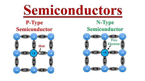
Table of Contents
N-Type Semiconductor vs. P-Type Semiconductor: A Deep Dive into the Differences
The world of electronics hinges on the remarkable properties of semiconductors. These materials, neither fully conductive like metals nor completely insulating like non-metals, form the backbone of modern technology. Crucially, their behavior can be meticulously controlled by introducing impurities, a process known as doping. This leads to two fundamental types: N-type and P-type semiconductors. Understanding the differences between these types is essential for grasping the functionality of transistors, diodes, and integrated circuits – the building blocks of all electronic devices.
What is a Semiconductor?
Before delving into the distinctions between N-type and P-type semiconductors, let's establish a foundational understanding of semiconductors themselves. Semiconductors are materials with electrical conductivity intermediate between that of conductors (like copper) and insulators (like rubber). Their conductivity is highly sensitive to temperature, light, and the presence of impurities. This sensitivity allows us to manipulate their electrical properties, making them ideal for electronic applications. Common semiconductor materials include silicon (Si), germanium (Ge), and gallium arsenide (GaAs).
Intrinsic Semiconductors: The Pure State
In their purest form, semiconductors are known as intrinsic semiconductors. In these materials, the number of electrons in the conduction band (free to move and carry current) is equal to the number of holes in the valence band (electron vacancies that act as positive charge carriers). At absolute zero temperature, all electrons reside in the valence band, rendering the material an insulator. However, as temperature rises, some electrons gain enough energy to jump from the valence band to the conduction band, leaving behind holes. This creates a balance between electron and hole carriers, contributing to a small but measurable conductivity.
Doping: The Key to Functionality
The true power of semiconductors emerges through doping – intentionally introducing impurities into the crystal lattice of the intrinsic semiconductor. This process dramatically alters the material's electrical properties. Two primary types of dopants exist:
- N-type dopants: These introduce extra electrons into the conduction band, increasing the number of negative charge carriers.
- P-type dopants: These create extra holes in the valence band, increasing the number of positive charge carriers.
Let's explore each in detail:
N-Type Semiconductors: A Sea of Electrons
N-type semiconductors are created by doping an intrinsic semiconductor with pentavalent impurities (atoms with five valence electrons). Common examples include phosphorus (P), arsenic (As), and antimony (Sb). When these impurities are introduced into the silicon crystal lattice, four of their valence electrons bond with neighboring silicon atoms, while the fifth electron is loosely bound and readily becomes a free electron in the conduction band. This extra electron isn't bound to a specific atom and can easily move through the material, contributing to its increased conductivity.
Key Characteristics of N-Type Semiconductors:
- Majority Carriers: Electrons are the majority carriers.
- Minority Carriers: Holes are the minority carriers.
- Dopant Atoms: Pentavalent (5 valence electrons).
- Conductivity: High conductivity due to the abundance of free electrons.
- Symbol Representation: Often represented by a circle with a '+' sign inside, representing the extra electron donated to the lattice.
P-Type Semiconductors: A Realm of Holes
P-type semiconductors are formed by doping an intrinsic semiconductor with trivalent impurities (atoms with three valence electrons). Boron (B), aluminum (Al), and gallium (Ga) are commonly used. When these impurities are introduced, they bond with three silicon atoms, leaving a "hole" – a vacant space where an electron should be – in the valence band. This hole acts as a positive charge carrier. A nearby electron can move into this hole, leaving behind another hole. This process effectively allows the "hole" to move through the lattice, contributing to conductivity.
Key Characteristics of P-Type Semiconductors:
- Majority Carriers: Holes are the majority carriers.
- Minority Carriers: Electrons are the minority carriers.
- Dopant Atoms: Trivalent (3 valence electrons).
- Conductivity: High conductivity due to the abundance of holes.
- Symbol Representation: Often represented by a circle with a '-' sign inside, indicating the absence of an electron (a hole).
The Crucial Difference: Charge Carriers
The fundamental difference between N-type and P-type semiconductors lies in their majority charge carriers:
- N-type: Majority carriers are electrons (negatively charged).
- P-type: Majority carriers are holes (positively charged).
This difference in charge carriers is what allows for the creation of P-N junctions, the basis of diodes and transistors. When N-type and P-type semiconductors are brought into contact, a depletion region forms, creating a unidirectional current flow – a fundamental concept in electronics.
Applications of N-type and P-type Semiconductors
The versatility of N-type and P-type semiconductors makes them indispensable in countless electronic applications:
N-type Semiconductor Applications:
- Transistors: N-type silicon is crucial in the construction of NPN bipolar junction transistors (BJTs), a fundamental building block of digital circuits.
- MOSFETs: N-type silicon is also utilized in n-channel metal-oxide-semiconductor field-effect transistors (MOSFETs), another prevalent transistor type.
- Integrated Circuits: N-type materials play a vital role in the intricate designs of integrated circuits (ICs), forming the basis of processors, memory, and other components.
- Solar Cells: N-type semiconductors are used in various solar cell designs to facilitate electron transport and enhance energy conversion efficiency.
- Resistors: N-type materials can be used in constructing resistors with specific resistance values within integrated circuits.
P-type Semiconductor Applications:
- Transistors: P-type silicon is essential for PNP BJTs and p-channel MOSFETs.
- Diodes: The P-N junction, a critical component in diodes, requires both P-type and N-type semiconductors. Diodes are used for rectification, voltage regulation, and signal processing.
- LEDs: Light-emitting diodes (LEDs) rely on the recombination of electrons and holes at the P-N junction, producing light. The specific semiconductor material determines the color of the emitted light.
- Solar Cells: P-type materials are a cornerstone in the design and fabrication of many types of solar cells.
- Integrated Circuits: Similar to N-type, P-type semiconductors are essential components in the complex architecture of integrated circuits.
Comparing N-type and P-type Semiconductors: A Summary Table
| Feature | N-Type Semiconductor | P-Type Semiconductor |
|---|---|---|
| Majority Carriers | Electrons | Holes |
| Minority Carriers | Holes | Electrons |
| Dopant Type | Pentavalent (e.g., Phosphorus, Arsenic) | Trivalent (e.g., Boron, Aluminum) |
| Charge Carriers | Negative | Positive |
| Conductivity | High | High |
| Symbol | Circle with '+' inside | Circle with '-' inside |
Beyond the Basics: Advanced Concepts
The differences between N-type and P-type semiconductors are fundamental to understanding numerous advanced concepts in semiconductor physics and electronics. These include:
- PN Junctions: The formation of a depletion region and the resulting rectifying properties are critical for understanding diodes and transistors.
- Carrier Concentration: The density of electrons and holes significantly impacts the semiconductor's electrical characteristics.
- Fermi Level: The Fermi level, representing the energy level at which there's a 50% probability of finding an electron, is different in N-type and P-type materials.
- Mobility: The ease with which electrons and holes move through the material is a critical parameter influencing the semiconductor's conductivity.
- Diffusion and Drift: Understanding how charge carriers move under the influence of concentration gradients (diffusion) and electric fields (drift) is crucial for analyzing semiconductor behavior.
Conclusion
N-type and P-type semiconductors are the cornerstones of modern electronics. Their contrasting properties – stemming from the introduction of specific dopants – enable the creation of a wide array of devices. Understanding the differences between these two fundamental semiconductor types is key to comprehending the inner workings of transistors, diodes, and integrated circuits, paving the way for a deeper understanding of the technology that permeates our daily lives. The detailed study of these materials continues to drive advancements in electronics, shaping the future of computing, communication, and numerous other fields.
Latest Posts
Latest Posts
-
Are Temperature And Volume Directly Proportional
Apr 01, 2025
-
Is Hydrogen More Electronegative Than Oxygen
Apr 01, 2025
-
What Happens When An Atom Gains Or Loses An Electron
Apr 01, 2025
-
How To Name Ionic And Covalent Bonds
Apr 01, 2025
-
Liquid In A Liquid Solution Example
Apr 01, 2025
Related Post
Thank you for visiting our website which covers about N Type Semiconductor Vs P Type Semiconductor . We hope the information provided has been useful to you. Feel free to contact us if you have any questions or need further assistance. See you next time and don't miss to bookmark.
